Lets start by build an amplifier;
I don't expect that you know how to design the amplifier yourself (that's why you're here?), so I'll hold your hand all the way through the design process, we'll be using at least one of the components in a way that I haven't described that it could be used like that yet, so there will be a little deviation to describe that, but hey, this is only lab3 and you're already building something pretty cool... you know the components from the past 5 lessons, and you're aware of one of the building blocks that we'll be using from a past lab lesson (lab 1).
Perhaps the holly grail of all analogue circuits is the amplifier, I don't know why if I'm honest, but just about everyone seems to want to know how to make amplifiers, and those that do know how to make amplifiers, well, in spite of the maths involved seem to get a kick out of making them, and even those that shy away from the maths have a really good go following reference circuits.
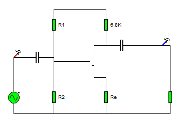
This is the first amplifier circuit I was ever introduced to:
Common Emitter Amplifier
The last amplifier that we looked at was an emitter follower or common collector amplifier, that's a device that amplifies current, whilst leaving voltage unchanged, we used that to boost the amount of current available from a low power source so that we could turn on a light.
The amplifier that we'll be looking at now doesn't amplify current, it amplifies voltage.
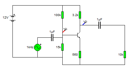
The first thing to do is introduce you to the circuit.
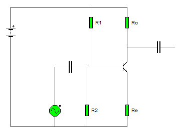
Firstly, lets break the circuit down,
The little round thing with the waveform shape in it is a signal source,
For this demonstration we'll set the output of the generator to a sine wave, with a frequency of 1KHz and we'll set the amplitude (size of the signal) to 1v.
This means that the waveform outputted by this generator is:
A nice curvy wave form, that is modelled by the math function sin(x).
It goes between +1v and -1v.
And it does this one thousand times a second (a complete cycle take 1millisecond -1ms.)
The next component we see is a capacitor, in the lesson on capacitors I talked about the capacitor acting like a storage tank for electricity, saying that you could charge a capacitor and discharge a capacitor, here we are using a different property of the capacitor, it's ability to block DC (direct current) signals, and allow AC (alternating current) to pass.
The reason that we want to use this is because we need to set a bias on the transistor so that it's working in a linear region, -don't worry about that for now, I'll explain more later, right now we'll look at the DC blocking capabilities of the capacitor.
When we use a capacitor like this it's called a coupling capacitor.
Coupling capacitors
The problem with the signal source that we have is that it's waveform is centred around 0volts.
fair enough the transistor will turn on then the voltage rises above zero volts, but when it's in it's negative half of the cycle (or anywhere in the cut-off region), the transistor won't be conducting at all. So we need to move the centreline of the wave form up so that it's centred around a positive voltage, that'll let our transistor work in a region where it's on a little right up to on a lot, (remember how we talked about the transistor as a variable switch? now we're going to use it as a variable switch.)
Before we introduce the transistor into the mix we'll look at how we get that wave form to climb up to a more positive voltage using coupling capacitors.
The diagram below shows some things that should be familiar to you from lab 1.
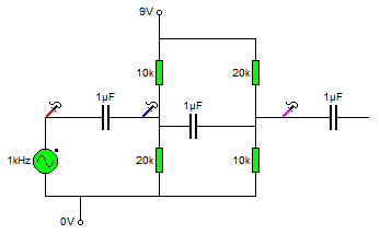
Ignore the capacitors and signal generator for now.
There is a positive voltage source (+9v) and a zero voltage source (0v) (just like the battery terminals.) And there are two resistors set up as a potential divider, followed by two more resistors set up as potential dividers.
Using the maths learned in Lab 1 we can see that the voltage at the blue probe is 6v, and the voltage at the pink probe will be 3v. -remember Vout = (Z2/(Z1+Z2)) * Vin)?
So we know that there is a DC voltage of 6v at the blue probe, and a DC voltage of 3v at the pink probe.
(now we'll include the capacitors and signal source again).
The resistors used are significantly high enough to not interfere with the source when the AC signal is introduced.
Reading from left to right.
The first red probe, measures voltage a +/-1v centred around 0v.
The capacitor then blocks any DC voltage going to, or from that point in the circuit moving onto the next point, (blue probe).
If there were no DC component here we'd measure +/- 1v centred around 0v, however, the potential divider here means that there is a 6v DC voltage at this point, so that +/-1v is superimposed on this 6v source. meaning that the wave form is now alternating between +7v and +5v (+/-1v centred around 6v).
Moving a little further on there is another capacitor that stops this +6v DC component from moving to or from any other part of the circuit. Here we reach the pink probe.
Now the wave form has had all it's DC component removed and is once again 0v +/-1v.
but our potential divider has set a DC voltage of 3v onto this part of the circuit. So once again the AC voltage is superimposed on the DC voltage giving a wave form that's +/- 1v centred around 3v (+4v to +2v).
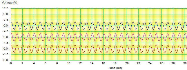
Here is what the wave forms are looking like at each part of the circuit.
Biasing
I suppose that the first question that needs to be answered is Why do we bias amplifiers. I gave a pretty poor description above about the fact that it doesn't turn on on the negative half cycle of the input wave, (and that is true).
but to answer the question properly again we're going to need to look at the data sheets for the component again.
Lets take a really simple (and now really rather old transistor, the BC108).
http://www.datasheetcatalog.org/datasheet/MicroElectronics/mXuvuyv.pdf
As before there are a couple of important things to look at in the data sheet.
The first is Base - Emitter voltage (Vbe) you can see that this is 0.6v

Next look at the gain value of the transistor, (this is called hfe) this is (for group A components typically 170).
this large hfe value means that we know that the collector current is much much larger than the base current.
so Vbe = 0.6
Gain = large
Ic >> Ib
Ie = Ic + Ib
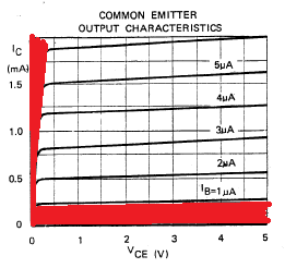
You'll find a graph in that data sheet called "output characteristics",
The output characteristics these define the voltages that you need across the device to make it work in a region called the linear region, this is the region where the device is going to amplify small and large signals equally without distorting either.
There are several lines on the device, all are in a shape that goes up at the start, and has a sharp knee, then settle into a straight line, the different line correspond to different base currents.
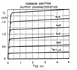
On the graph below I've marked two areas in red, you want to stay out of these regions because either the transistor is off or behaving in a non linear way (very on), (the one closest to the X axis is the cut off region) and the one closest to the Y axis is the saturation region.
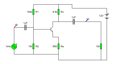
The first thing that you're going to need to determine is the Resistor RL, this is the load resistor for the amplifier,
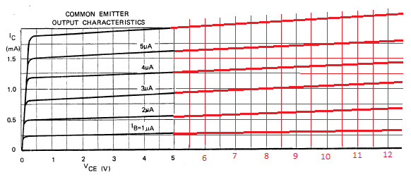
First, you're going to need to extend the graph so that we can see it working inside the voltages that you're working with, (the x axis only goes up to 5v, and we're going to use a 12volt supply).
(I'll assume by now that you've murdered an ATX power supply and therefore have a 12v supply (and are no longer relying on 9v batteries).
Now you need to draw line on the graph between the point the you want to set as ICmax, (on the Y axis, and your supply voltage (Vcc) on the X axis.
Set your ICmax somewhere below the highest marking on the chart, I've chosen 1.75mA
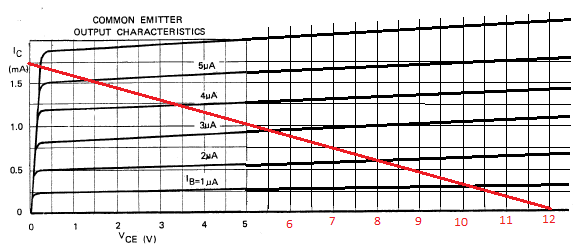
This new red line is called the DC load line, and in the middle of this line is a point that's at the middle of the linear operating region of the amplifier, this is the quiescent point, or Q point.
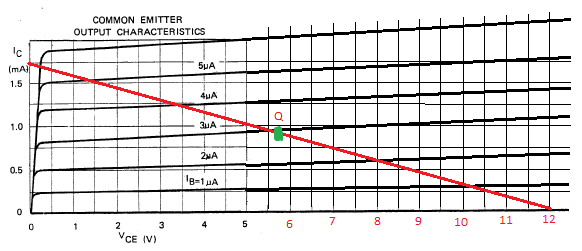
You can see the green dot in the middle, set at around 5.8v (you might also be realising that this is not an exact science!)
Right... so what we know now is:
Ic(max) = 1.75mA
and Vcc = 12
Vce(q) = 5.8
Ic(q) = 0.9mA
We need to make a decision now as to what we want the voltage of our emitter to sit at, some guides suggest splitting the voltage equally between the Rc, Rb and the transistor itself, however, I think that setting Vre as 1v doesn't seem like a terribly bad thing to do! -you could chose a different value.
To find a value for Rc
We use the forumla
Ic(max) = (Vcc - Vre)/Rl
0.00175 = (12 - 1)/Rl
Which works through to give us the equation
Rl = 11/0.00175 = 6285
The closest standard value is 5.6K or 6.8K
It'll be perfectly fine to use a 5.6K this will increase your IC(max) value, but you're still far below the absolute maximum rating given on the first page of the data sheet. the higher the voltage here the more restrictive you're being on the input signal voltages that could be used before the amplifier clips the signal.
The current gain of the transistor we know from the data sheet is 170
the gain is the value of the collector current, over the base current
hfe = Ic /Ib
hfe = 170 and Ic = 1.75mA
Therefore Ib = 1.75ma / 170 = 10uA
Given that we now know the values of Vre, Vbe and Ib we can start to set the bias of the base leg of the transistor.
To find the value of R2 we use the following formula.
R2 = (Vre + Vbe)/(10 * Ib)
R2 = (1 + 0.6)/10 * 0.00001)
R2 = 1.6/100 * 100^-6 = 16000 -15k is the closest standard value
and we can also figure out the value for R1
R1 = (Vcc -(Vre + Vbe))/(11*Ib)
R1 = (12 - 1.7)/(11*0.00001)
R1 = 10.3/0.00011 = 93636 - 100k is the closest value
Now we need to go about setting that emitter resistor Re.
We calculate this using Ohms law
We know that the emitter current is the sum of the base and collector current
Ie = Ic + Ib
Ie = 1.75ma + 10uA
Ie = 1.76mA
We know that Ohms law says V/I = R
Vre / Ie = Re
1 / 1.76mA
1/0.00176 = 568 Ohms (and the closest standard value is 560Ohms)
Earlier we talked about coupling capacitors,
on that last amp circuit you'll see red and blue probes, this is what the signal looks like at those points.
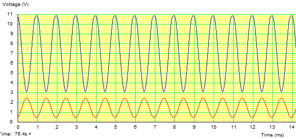
Input vs. Output
Finally, let's move our probes to measure the input and output signals.
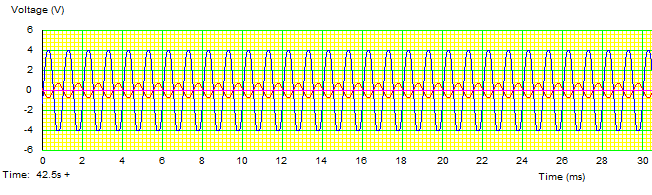
Look closely at that chart.
The red line is the input signal, and the blue line is the output. We see that the blue line is much bigger than the red line, but also notice that as the red line is going up, the blue line is going down.
This amplifier has switched this signal upside down.
This type of amplifier is called an inverting amplifier.
Gain
The gain of am amplifier is its output divided by its input.
remember the current gain of the transistor was the collector current, over the base current.
(actually it's emitter current over the base current, but since the gain factor is so large we assume that Ie is just about equal to Ic)
The voltage gain works the same.
The input voltage is +/-1v, (e.g 2v).
and the output voltage swing is +/- 4v (eg 8v)
So the gain of this amplifier is 8/2 = 4
The signal coming in is made 4 times larger.
No comments:
Post a Comment